
So far in our processor design we created an assembler in VHDL in part 1 and designed a processor with configurable word lengths in part 2 and we designed it to have configurable number of pipelines in part 3. The processor was designed to do basic floating point add, sub and multiply instructions between registers and we used it to calculate a first order filter. In this part we will continue improving on the design and modify it to bypass the register load and store stages entirely and instead operate directly on the memory contents by inserting the float alu after the memory load stage and making our instructions reference ram directly.
With direct memory interfacing we can fetch data from memory, then operate with it and lastly push it back to memory with a single instruction. This massively increases the efficiency of our floating point processing as we can now more easily keep the processing pipeline filled with instructions. To make it easy to keep our pipeline filled with instructions, we will also add a function to our VHDL assembler which allows us easily write pipelined code sections in VHDL directly. The assembler takes the form of functions that allow us to input instructions and it converts them to bit vectors that are then processed in the processing pipeline which greatly simplifies simulation and implementation of simple programs.
The assembler and processor design is tested with Efinix Titanium, Intel Cylone 10lp, Lattice ECP5 and AMD Artix 7 all of which are running their respective minimum pipeline depths to meet 120MHz timing of our example design. The example creates a noisy sine wave which is filtered with the bank of filters. The results are then read back from the fpga using uart. All sources can be found from hVHDL github page and the example project, the processor as well as the memory and floating point are in separate repositories and included in the example project as git submodules for easy reuse.
Processing directly from FPGA ram
A processor essentially is a ram which stores the instructions and data, aa program counter to keep track of the ram address that we are reading the instructions from and a processing pipeline to which we push the instructions are read from ram.
Since we use the hVHDL project libraries, all of which have subroutine interfaces, our ram reader and the instruction pipeline can be built with just a handful of lines of VHDL. Assuming that we have put all of our processor registers in a record, the following snippet gives us an instruction pipeline that gets filled with instructions from ram. You can find the full package in the hVHDL microprogram processor repository
    if rising_edge(clock) then
        init_ram(ram_read_instruction_in, ram_read_data_in, ram_write_port);
        ------------------------------------------------------------------------
        processor.program_counter <= processor.program_counter + 1;
        request_data_from_ram(ram_read_instruction_in, processor.program_counter);

        if ram_read_is_ready(ram_read_instruction_out) then
            used_instruction := get_ram_data(ram_read_instruction_out);
        else
            used_instruction := nop;
        end if;

        processor.instruction_pipeline <=
            used_instruction & self.instruction_pipeline(0 to processor.instruction_pipeline'high-1);
The lines 13 and 14 form the instruction pipeline. The instruction pipeline is an array of registers that shift the data forward by one register on each clock cycle and these are the registers from which we operate our instructions from.
Register processing pipeline
Previously the float alu procedures were called based on the decoded instructions directly as shown below
            CASE decode(processor.instruction_pipeline(0)) is
                WHEN load =>
                    request_data_from_ram(ram_read_data_in, get_sigle_argument(used_instruction));
                WHEN add =>
                    add(float_alu,
                        to_float(self.registers(get_arg1(used_instruction))),
                        to_float(self.registers(get_arg2(used_instruction))));
                WHEN mpy =>
                    multiply(float_alu,
                        to_float(self.registers(get_arg1(used_instruction))),
                        to_float(self.registers(get_arg2(used_instruction))));
                ---
In order to process some data from memory, we were first loading the data onto a register and then the register contents were added, subtracted or multiplied together and lastly the data was pushed from register back to memory. The float alu could only reach the registers which needed to be interfaced to ram with separate instructions. If we were processing a stream of data we would need to interrupt the processing for loading new data onto the registers from ram.
To make our new processing pipeline run directly off of memory we just need to change the first decoding stage such that the instructions reference ram addresses instead of registers. To make it work we move the procedure calls for the float alu up a few instruction pipeline stages to where the data has been read from ram.
Memory processing pipeline
Since we now put the memory into the pipeline, the instruction processing gets split into two separate stages. In the first stage we request data from ram based on the decoded arguments and in the second part we feed the data from ram ports to the floating point alu directly as follows
            --stage 0
            CASE decode(processor.instruction_pipeline(0)) is
                WHEN add =>
                    request_data_from_ram(ram_read_data_in   , get_arg1(used_instruction));
                    request_data_from_ram(ram_read_2_data_in , get_arg2(used_instruction));
                WHEN sub =>
            ---

           --stage 2, -- memory is ready here
            CASE decode(processor.instruction_pipeline(2)) is
                WHEN add =>
                    add(float_alu
                        to_float(get_ram_data(ram_read_data_out)) ,
                        to_float(get_ram_data(ram_read_2_data_out)));
In the other end of the pipeline when the alu is ready, the destination gets decoded and the data is written back to ram based on the decoded destination address.
            used_instruction := self.instruction_pipeline(ram_latency + alu_timing.madd_pipeline_depth-1);
            CASE decode(used_instruction) is
                WHEN add | sub | mpy | mpy_add =>
                    write_data_to_ram(ram_write_port, get_dest(used_instruction), to_std_logic_vector(get_result(float_alu)));
                WHEN others => -- do nothing
            end CASE;
The entire memory processing pipeline is just the following 64 lines of code
            create_simple_processor (
                self                     ,
                ram_read_instruction_in  ,
                ram_read_instruction_out ,
                ram_read_data_in         ,
                ram_read_data_out        ,
                ram_write_port           ,
                used_instruction);

            init_ram_read(ram_read_2_data_in);
            init_ram_read(ram_read_3_data_in);
            create_float_alu(float_alu);

            --stage -1
            CASE decode(used_instruction) is
                WHEN add =>
                    request_data_from_ram(ram_read_data_in   , get_arg1(used_instruction));
                    request_data_from_ram(ram_read_2_data_in , get_arg2(used_instruction));
                WHEN sub =>
                    request_data_from_ram(ram_read_data_in   , get_arg1(used_instruction));
                    request_data_from_ram(ram_read_2_data_in , get_arg2(used_instruction));
                WHEN mpy =>
                    request_data_from_ram(ram_read_data_in   , get_arg1(used_instruction));
                    request_data_from_ram(ram_read_2_data_in , get_arg2(used_instruction));
                WHEN mpy_add =>
                    request_data_from_ram(ram_read_data_in   , get_arg1(used_instruction));
                    request_data_from_ram(ram_read_2_data_in , get_arg2(used_instruction));
                    request_data_from_ram(ram_read_3_data_in , get_arg3(used_instruction));
                WHEN others => -- do nothing
            end CASE;
        ------------------------------------------------------------------------
            --stage 2
            used_instruction := self.instruction_pipeline(2);

            CASE decode(used_instruction) is
                WHEN add =>
                    madd(float_alu                                ,
                        to_float(1.0)                             ,
                        to_float(get_ram_data(ram_read_data_out)) ,
                        to_float(get_ram_data(ram_read_2_data_out)));
                WHEN sub =>
                    madd(float_alu                                  ,
                        to_float(-1.0)                              ,
                        to_float(get_ram_data(ram_read_2_data_out)) ,
                        to_float(get_ram_data(ram_read_data_out)));
                WHEN mpy =>
                    madd(float_alu                                  ,
                        to_float(get_ram_data(ram_read_data_out))   ,
                        to_float(get_ram_data(ram_read_2_data_out)) ,
                        to_float(0.0));
                WHEN mpy_add =>
                    madd(float_alu                                  ,
                        to_float(get_ram_data(ram_read_data_out))   ,
                        to_float(get_ram_data(ram_read_2_data_out)) ,
                        to_float(get_ram_data(ram_read_3_data_out)));
                WHEN others => -- do nothing
            end CASE;
        ----------------------
            used_instruction := self.instruction_pipeline(ram_latency + alu_timing.madd_pipeline_depth-1);
            CASE decode(used_instruction) is
                WHEN add | sub | mpy | mpy_add =>
                    write_data_to_ram(ram_write_port, get_dest(used_instruction), to_std_logic_vector(get_add_result(float_alu)));
                WHEN others => -- do nothing
            end CASE;
Note that we have used madd, or multiply-add instruction for all of the 4 basic arithmetic operations. The multiply-add evaluates a\cdot x + b operation. Using the same operation for all math instructions simplifies the design as now all instructions take same amount time to propagate through the pipeline without any additional design effort.
Looking at the memory processing pipeline above, the stage of the instruction pipeline where the data is captured from the float alu is read from position ram_latency + alu_timing.madd_pipeline_depth-1. These constants are used to define depth of our float alu pipeline. These constants are part of the float alu library and they allow us to change the float alu pipelining and the processor will automatically get configured to read the result at the correct point of the pipeline.
For our 32 bit instructions we have 4 bits for the commands and our instructions can have 7 bit argument and destination fields. With 7 bits we can reference up to 128 different memory locations for inputs and outputs of our instructions. The instructions are designed as shown below
    subtype comm is std_logic_vector(31 downto 28);
    subtype dest is std_logic_vector(27 downto 21);
    subtype arg1 is std_logic_vector(20 downto 14);
    subtype arg2 is std_logic_vector(13 downto 7);
    subtype arg3 is std_logic_vector(6 downto 0);
To access more memory than what can point with our 32 bit instructions, we could add a register to load the upper bits of the memory addresses to. This way we could have a register which gives us access to specific 128 memory locations in the memory. We could also arrange the data into the memory differently so that we would not need to have full random access to all parts of the memory.
Assembling pipelined instructions in VHDL
Since our processing pipeline and float alu can handle configurable pipeline depths, we want to be able to write our software also in a way that it works with any length instruction pipeline.
The effect of pipelining in a processor instructions is shown in the snippet below. The code first calculates a subtraction between u and y and puts it into temp. The mpy_add instruction then uses the result of the sub instruction from temp.
            write_instruction(sub  , temp , u    , y) -- temp <= u - y
            write_instruction(nop)
            write_instruction(nop)
            write_instruction(mpy_add , y , temp , g, y) -- y <= (temp*g) + y
            write_instruction(nop)
            write_instruction(nop)
            write_instruction(program_end)
If we assume that there are 2 pipeline stages in the sub instruction there needs to be 2 wait states, or instructions between the sub and the mpy_add. This is needed so that the sub operation has had enough time to pass through its pipeline so that the result can be used by the mpy_add instruction.
It does not actually matter what we put into those pipeline stages as we only care about the delay between sub and mpy_add instructions. We can for example run two additional low pass filters in the pipeline stages of the filter as seen here
            write_instruction(sub, temp  , u, y) -- temp <= u - y
            write_instruction(sub, temp2 , u, y1)
            write_instruction(sub, temp3 , u, y2)
            write_instruction(mpy_add , y , y , g , temp) -- y <= (temp*g) + y
            write_instruction(mpy_add , y2, y2, g2, temp2)
            write_instruction(mpy_add , y3, y3, g3, temp3)
            write_instruction(nop) -- first filter is ready here
            write_instruction(nop) -- second filter is ready here
            write_instruction(nop) -- third filter is ready here
As long as we have instructions to push into the pipeline, we are not wasting any processing time.
Working with configurable pipeline depths
In part 3 we made our processor to have configurable pipeline depths which allows us to add or remove registers to meet timing. Therefore we need to make sure our software works with different pipeline depths and this is developed next.
We can think of the code snippet as being two blocks of pipelineable instructions
            block(
                write_instruction(sub, temp  , u, y) -- temp <= u - y
                write_instruction(sub, temp2 , u, y1)
                write_instruction(sub, temp3 , u, y2)
            )
            block(
                write_instruction(mpy_add , y , y , g , temp) -- y <= (temp*g) + y
                write_instruction(mpy_add , y2, y2, g2, temp2)
                write_instruction(mpy_add , y3, y3, g3, temp3)
            )
The second block can only be started when the result from first instruction of the first block is available for the first instruction of the second block. What we want to have is a function that can take in the array of instruction of the block that we want to process and fills in the nop instructions if and when needed so the second block starts when the data is ready.
In the pipeline_block function below, we use the return value variable. This is an an array of instructions which has length of the processors processing pipeline and which is populated with nop instructions. The body of the function then compares the length of the program array which is passed into the function to the length of the return value. If the program is shorter, the program is copied to the retval and the return value is returned and if the program’length is equal or longer than the processing pipeline, then the program that was passed in is returned directly.
    function pipeline_block
    (
        program : program_array
    )
    return program_array
    is
        variable retval : program_array(0 to number_of_pipeline_stages-1) := (others => write_instruction(nop));
    begin

        if program'length < retval'length then
            for i in program'range loop
                retval(i) := program(i);
            end loop;
            return retval;
        else
            return program;
        end if;

    end pipeline_block;
The result of this function is then expanded into our design with the nop commands inserted to pad the pipeline when necessary. Wrapping a pipelineable block of instructions with this pipeline_block function thus guarantees that the first instruction of the next block will be reading memory that is written by the first instruction of the previous block regardless of the pipeline depth.
Test code
To test our memory processor design we will rewrite our first order filter example which we used in previous parts to use these sequential blocks. In the first pipeline block below we are triggering the subtraction of 10 filters in successive clock cycles. In the second sequential block the outputs of the 10 filters are calculated concecutive calls to the mpy_add function.
The function takes in the filter gain and then scales it up to create 10 copies of the filter with progressively higher gains. The
   function build_nmp_sw (filter_gain : real range 0.0 to 0.1; u_address, y_address, g_address, temp_address : natural) return ram_array
    is

        ------------------------------
        constant program : program_array :=(
            pipeline_block(
                program_array'(write_instruction(sub, temp_address, u_address, y_address)    ,
                write_instruction(sub, temp_address+1, u_address, y_address+1) ,
                write_instruction(sub, temp_address+2, u_address, y_address+2) ,
                write_instruction(sub, temp_address+3, u_address, y_address+3) ,
                write_instruction(sub, temp_address+4, u_address, y_address+4) ,
                write_instruction(sub, temp_address+5, u_address, y_address+5) ,
                write_instruction(sub, temp_address+6, u_address, y_address+6) ,
                write_instruction(sub, temp_address+7, u_address, y_address+7))
            ) &
            pipeline_block(
                program_array'(write_instruction(mpy_add, y_address, temp_address, g_address, y_address) ,
                write_instruction(mpy_add, y_address+1, temp_address+1, g_address+1, y_address+1) ,
                write_instruction(mpy_add, y_address+2, temp_address+2, g_address+2, y_address+2) ,
                write_instruction(mpy_add, y_address+3, temp_address+3, g_address+3, y_address+3) ,
                write_instruction(mpy_add, y_address+4, temp_address+4, g_address+4, y_address+4) ,
                write_instruction(mpy_add, y_address+5, temp_address+5, g_address+5, y_address+5) ,
                write_instruction(mpy_add, y_address+6, temp_address+6, g_address+6, y_address+6) ,
                write_instruction(mpy_add, y_address+7, temp_address+7, g_address+7, y_address+7))
            ) &
            write_instruction(program_end));
        ------------------------------
        variable retval : ram_array := (others => (others => '0'));

    begin

        for i in program'range loop
            retval(i) := program(i);
        end loop;

        retval(y_address) := to_std_logic_vector(to_float(0.0));
        retval(u_address) := to_std_logic_vector(to_float(0.5));
        for i in 0 to 9 loop
            retval(g_address+i) := to_std_logic_vector(to_float(filter_gain + filter_gain*(real(i))));
        end loop;

        return retval;

    end build_nmp_sw;
The output of the build_nmp_sw is the ram memory contents that are then given to the multi-port ram initial values through the generic map.
-- in architecture
    constant u_address : natural := 80;
    constant y_address : natural := 90;
    constant g_address : natural := 100;
    constant temp_address : natural := 110;

    -- program is stored in a constant
    constant ram_contents : ram_array := build_nmp_sw(0.05 , u_address , y_address , g_address, temp_address);
begin

    process(clock)
    begin
        if rising_edge(clock) then
            -- instantiate processor and processing pipeline
        end if;
    end process;

------------------------------------------------------------------------
    u_mpram : entity work.ram_read_x4_write_x1
    generic map(ram_contents) -- program is given to memory as generic
    port map(
    clock                    ,
    ram_read_instruction_in  ,
    ram_read_instruction_out ,
    ram_read_data_in         ,
    ram_read_data_out        ,
    ram_read_2_data_in       ,
    ram_read_2_data_out      ,
    ram_read_3_data_in       ,
    ram_read_3_data_out      ,
    ram_write_port);
Fpga implementation

The floating point module is tested with a noisy sine that is then filtered using the floating point filter. The project has build scripts for Intel Quartus, Lattice Diamond, Xilinx Vivado and Efinix Efinity. Both the Efinix and Lattice tools need the newest versions of the tools for the code to work. The VHDL sources for the example project can be found in github and the floating direct memory processor implementation specifically can be found here. The sine wave is calculated using the sincos module that was been designed previously.
The memory processor is added to the test project alongside the fixed and floating point filters and the previously designed processor. The main process of the project initializes the filter and processor modules, creates the sine and noise and triggers the modules. The full source for the main module can be found here.
create_noisy_sine : process(system_clock)
    begin
        if rising_edge(system_clock) then
            init_example_filter(floating_point_filter_in);
            init_example_filter(fixed_point_filter_in);
            init_example_filter(mcu_in);
            init_example_filter(mcu_in2);

            increment_to(i, limit_for_100khz);

            if i = 0 then
                angle    <= (angle + 10) mod 2**16;
                calculate_prbs(prbs7);

                request_sincos(sincos, angle);

            end if;

            if sincos_is_ready(sincos) then
                sine_with_noise <= get_sine(sincos) + to_integer(signed(prbs7)*64);
                request_example_filter(floating_point_filter_in , sine_with_noise);
                request_example_filter(fixed_point_filter_in    , sine_with_noise);
                request_example_filter(mcu_in                   , sine_with_noise);
                request_example_filter(mcu_in2                  , sine_with_noise);
            end if;
        end if; --rising_edge
    end process;
------------------------------------------------------------------------
    u_floating_point_filter : entity work.example_filter_entity(float)
        generic map(filter_time_constant => filter_time_constant)
        port map(system_clock, floating_point_filter_in, bus_from_communications, bus_from_floating_point_filter);

---------------
    u_fixed_point_filter : entity work.example_filter_entity(fixed_point)
        generic map(filter_time_constant => filter_time_constant)
        port map(system_clock, fixed_point_filter_in, bus_from_communications, bus_from_fixed_point_filter);

---------------
    u_mcu : entity work.example_filter_entity(microprogram)
        generic map(filter_time_constant => filter_time_constant)
        port map(system_clock, mcu_in, bus_from_communications, bus_from_mcu);

---------------
    u_mcu2 : entity work.example_filter_entity(memory_processor)
        generic map(filter_time_constant => filter_time_constant, filter_output_address => 110)
        port map(system_clock, mcu_in2, bus_from_communications, bus_from_mcu2);

------------------------------------------------------------------------
------------------------------------------------------------------------
    combine_buses : process(system_clock)
    begin
        if rising_edge(system_clock) then
            bus_to_communications <= bus_from_interconnect          and
                                     bus_from_floating_point_filter and
                                     bus_from_fixed_point_filter    and
                                     bus_from_mcu                   and
                                     bus_from_mcu2;
        end if; --rising_edge
    end process combine_buses;
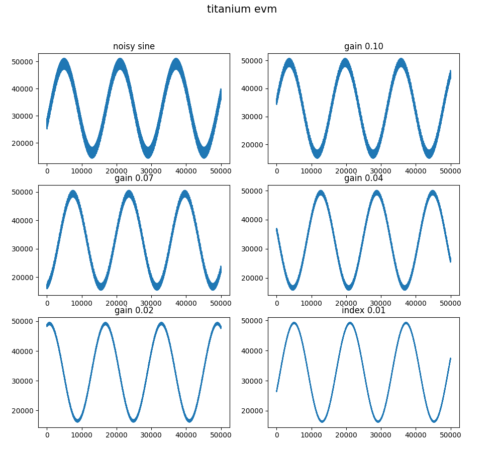
The filter results are accessed using an uart and there is a test_app.py python script through which the uart is accessed. Running the python script request 50k points of data from the unfiltered sine and then the outputs of the floating point filter from the memory processor corresponding with gains of 0.01, 0.02, 0.04, 0.07 and 0.1 which is shown in Figure 1 below.
The memory processor is instantiated in the same project with the register based processor to easily compare the synthesis results. Since the newly designed floating point processor does not use logic or registers for the register file, it is very efficient in its use of logic as shown below. The logic count calculates the logic that is inside the the processor entity so it has the integer to float and float to integer conversions, float alu, processor and the connections to the internal bus which is accessed using uart.
Resource use for direct memory processor with different fpgas
| FPGA(vendor) | DSP | LUT(reg) | Memory Block | Pipelines (norm/denorm) |
|---|---|---|---|---|
| Cyclone 10 lp(Intel) | 7(9x9bit) | 1497(1382) | 7(M9k) | 3/3 |
| Artix 7(AMD) | 2 | 663(669) | 2 bram, 15 dmem | 2/2 |
| ECP5 (Lattice) | 4 | 1007(983) | 4 ebr, 8 dmem | 2/2 |
| Certus NX(Lattice) | 4 | 1165(1132) | 4 ebr, 11 dmem | 4/4 |
| Titanium(Efinix) | 4 | 860(587) | 8(ram 10k) | 1/1 |
| Trion(Efinix) | 4 | 1100(1000) | 16(ram 5k) | 3/4 |
If we compare the resource use to the processor with 8 registers that were done using general logic fabric, we can see that the resource use has roughly been halved with the cost of doubling the memory use due to double amount of read ports.
Resource use for load-store processor with different fpgas
| FPGA(vendor) | DSP | LUT(reg) | Memory Block | Pipelines (norm/denorm) |
|---|---|---|---|---|
| Cyclone 10 lp(Intel) | 7(9x9bit) | 3514(1331) | 4(M9k) | 3/3 |
| Artix 7(AMD) | 2 | 1926(1365) | 1 bram, 59 dmem | 2/2 |
| ECP5(Lattice) | 4 | 3132(1273) | ebr 2, dmem 36 | 4/3 |
| Certus NX(Lattice) | 4 | 2826(1016) | ebr 2, dmem 11 | 4/4 |
| Titanium(Efinix) | 4 | 1972(910) | 3(10k) | 1/1 |
| Trion(Efinix) | 4 | 2570(1432) | 6(5k) | 3/4 |
Notes
Previously we have built a processor that can do basic floating point operations between registers. In part 1 we designed an assembler using VHDL and a simple processor to test the assembler. In part 2 we extended the processor such that we can use arbitrary word lengths and also run floating point arithmetic with it and in part 3 we added a possibility to configure the pipelining of the processor and tested it with several common FPGAs. The memory processor inherits all the traits from the previous designs, hence it has configurable pipeline depth, and we can parametrize the instruction set and instruction decoding and length.
With memory to memory processor architecture we have increased the latency of the processor pipeline by the amount of the memory operations but we can reach a lot more data directly with the instructions. The processor is also very efficient in its use of resources. The example project also has a single floating point filter done directly in logic and it uses almost exactly the same amount of logic resources as the floating point processor does and with the processor we calculate 10 filters instead of 1. The processor does not have branching or stalling instructions yet, but we will add those at some point.