
In our previous post we designed basic differential equation solvers which are really useful for when we are designing signal processing and control systems with FPGAs. In this blog we will design a VHDL simulation model for a Flying Capacitor 4-level Buck converter using the hVHDL_ode library. This switching model can be used for control development in VHDL directly. Designing a simulation model means deriving the output voltage equation as well a the capacitor charge equations and modulation for the converter and then integrating these equations with a differential equation solver. Lastly we run the VHDL simulation model of a 4-level flying capacitor converter and verify the model against a QSPICE simulation of the same circuit.
To build a simulation model for the flying capacitor converter we need a model for the flying capacitor currents as well as the converter output voltage and a stable modulation sequence which are developed in this blog. Together with the runge-kutta solver they allow us to run a simulation in vhdl that closely match the QSPICE simulation.
Duplicating the results in this blog
To run the QSPICE simulation, you need QSPICE. Additionally for the VHDL simulation you need VUnit python library and NVC simulator which you can install from powershell using
winget install --id NickGasson.NVC -e
pip install vunit-hdl
The way you can duplicate the simulation results shown in this post is by cloning the qspice_flying_cap repository with submodules and running 3 python scripts. The powershell commands to run both models and plot results is shown below.
git clone https://github.com/johonkanen/qspice_flying_cap.git --recurse-submodules
cd qspice_flying_cap
& 'C:\Program Files\QSPICE\dm\bin\dmc.exe' -mn -WD fc_4level_x1.cpp kernel32.lib
python .\run_fc4level.py
python hVHDL_ode\vunit_run_ode.py *ode*.*fc*.all
python .\plot_fc_4_level.py
First line is a call to dmc compiler which compiles the required .dll file for the modulator. DMC is shipped with QSPICE so you should have it installed already. The run_fc4level.py runs the QSPICE simulation model and saves the simulation results in a .csv . The call to vunit_run_ode.py runs the vhdl simulation which also writes a .dat file with simulation results. Lastly both of the simulation results are plotted in a single figure by the plot_fc_4_level.py
Flying Capacitor Converter
For common two level converters like buck and boost converters, we convert a steady DC voltage to variable voltage with a switching pattern. The DC voltage is chopped to pulses which have average voltage of corresponding to the reference voltage. The pulses have only 2 levels, either zero volts or output equal to the dc link voltage and this standard pulse width modulation. If we were modulating a 150V output from 300V DC link we would do a 50% pwm pattern to get average of half of dc link.

With a multilevel converter we can switch voltages that are between V_{dc} and 0 . For 3 levels we can switch dc, dc/2 and zero volts and for 4 level we can switch between 3/3\cdot V_{dc} , 2/3\cdot V_{dc} , 1/3\cdot V_{dc} and 0/3\cdot V_{dc} . If we have a 4 level converter with 300V dc link and we are modulating 150V we can do a 50% pwm pattern between 100V and 200V.

The simplest multilevel converter that is the 3-level flying capacitor converter is shown in Figure 3. The converter has series connected switches with a capacitor that is connected between the top and bottom side switches. The name of the converter comes from this extra capacitor which “flies” between zero and DC link.

A better way to draw the flying capacitor converter is shown below. Note that this is the exact same converter but the top and bottom side switches are just drawn in parallel rows. This is more intuitive layout as the complementary PWM switches are aligned and it is easier to trace the current path that corresponds with different switch states.
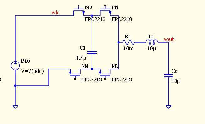
The possible switch states are determined by the high side switches M_2 and M_1 as M_3 is the complementary of M_1 and M_4 is complementary to M_2 . Thus with two high side switches there are 4 possible states that can be switched as shown in the table below
When both switches M_2 and M_1 conduct as indicated by the state \left[1,1 \right] , the inductor is connected directly to DC link and hence output voltage is V_{dc} . When both low side switches M_4 and M_3 in state \left[0,0 \right] conduct we get zero volts.
Now there are 2 other states that we can use, that is either \left[1,0 \right] or \left[0,1 \right] . In state \left[1,0 \right] the flying capacitor is connected beween DC link and output hence the voltage is V_{dc} – V_{C_1} and in \left[0,1 \right] output voltage is V_{C_1} .
If flying capacitor voltage is V_{dc}/2, then both states where the flying cap is connected have output equal to half of DC link. To keep the flying cap at V_{dc}/2 we can modulate the output voltage such that we alternate between the two midpoint states. This way the capacitor gets charged and discharged for equal amount of time in the switching cycle and is kept at the middle point of the dc link voltage. The switch states and corresponding bridge output voltages are tabulated below
From the table we can see that if the state is 01 the corresponding capacitor voltage is positive and if it is 10 it is negative. Both 11 or 00 bypass the capacitor and hence the voltage is multiplied by zero. The flying capacitor modulation algorithm that takes in two logic bit values and returns either +1, -1 , or 0 is
This simple algorithm can be used with arbitrary number of flying capacitor stages which we will show next.
Multi-Level Flying Capacitor Converters
Using the sideways layout allows us to draw more flying capacitor stages with just additional copies of the flying capacitor stage with 2 switches and a capacitor. Adding one stage we get 4-levels with 3 high side switches as shown in Figure 2.

With the sideways layout the way we can visually construct the output voltage and the capacitor charge equations. We do this by tracing the current route through the circuit with given switch state.
Here we have 4 level converter with the switch state 101. With this combination the current flows through DC link capacitor in the down-up direction which corresponds to positive voltage and discharging current, top-bottom in second flying cap resulting in negative voltage and charging current, and from bottom-up in the first flying cap resulting in positive voltage and discharging current. Hence we get the output voltage equation for 101 that is V_{dc}-V_{C_2}+V_{C_1} and the capacitor currents are i_{C_1} = -i and i_{C_2} = i correspondingly
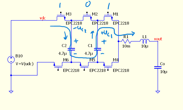
In a four level converter with 3 high side switches we have 2^3 = 8 possible switching states. Tabulating all binary values with the 3 high side switches and going through all of the switching states we get the following switching table. Note that I abuse the notation a bit and drop the V’s from the voltage to make the equations easier to look at and hence the voltages will be marked as 1-C_2+C_1 .
Since the flying capacitor voltages are charged C_1 = 1/3 and C_2 = 2/3 we get the output voltages equations as shown in the table below. Since the flying capacitor currents also equal just the sign swapped voltage equation we will drop the currents from the table now on
If we rearrange the table to align with the switched voltage levels we get a clearer view on the relation of switch states and output voltages
From the rearranged table we can see that the number of conducting high side switches corresponds with the index of the switched voltage. So if our modulated voltage is between 2/3 and 3/3 of the dc link voltage, the modulator needs to alternate between 2 conducting high side switches and 3 conducting high side switches.
Using the Flying Capacitor Modulation algorithm for a multi-level Flying Capacitor converter
With increasing number of levels, populating the switching table gets cumbersome by manually tracing the current paths, but with the modulation algorithm (1) we can relatively easily construct the switching table for arbitrary number of levels. The way we get the output equation directly from the state using the modulation algorithm (1) is by appending the switch state vector with a “phantom” zero and then going one switch at a time and check pairwise with the previous switch state the voltage of the capacitor. The last switch gives the DC link voltage equation, second to last switch gives the highest voltage capacitor equation and so on.
The output voltage equation for switch state 101 is constructed using this algorithm below. The table has the actual switch state vector and the sub vectors corresponding to each capacitor voltage separately
The method is consistent and can be used with switch states 111 and 000 also
Here is the 5 – level switching table constructed using the simple algorithm arranged with the switched output voltage levels.
Since the number of ones in the binary vector corresponds with the index of the switched voltage, the highest and lowest switched levels are always a square matrix with diagonal populated with zeros or ones correspondingly. Additionally, all the other intermediate stages are also populated using all possible combinations of ones in the switch state. Inverting all the bits in the vector also results in the complementary equation which we can observe in the table above.
Flying Capacitor Modulation
Now that we have the switching states and output voltage, we can next construct a modulation principle for the converter. We can actually use any arbitrary sequence of switch states, skipping voltage levels or just alternating between two states, but we need the sequence of states to stabilize the flying capacitors.
A stable modulation sequence is one which charges and discharges the flying capacitors for equal amount of time after some finite sequence of switched states. A stable switching sequence for a 4-level flying capacitor converter between 2/3 and 1/3 levels is tabulated below. Note that each switch transition is made by toggling a single switch so this would also be a sequence with minimal switch transitions.
We can also swap g_3 and g_2 columns and get another stable sequence with minimal switch transitions.
If we trace out the individual gate signals we can see that this corresponds to phase shifted PWM. All three gates are high for 3 units and low for 3 units. This results in a 50/50 PWM pattern between the 2/3 and 1/3 voltage levels.

Now with the flying capacitor current and output voltage algorithm and a stable modulation sequence, we can build a simulation model using a differential equation solver.
VHDL simulation of a 4-level flying capacitor converter
Since the flying capacitor converter is actually a controllable voltage source, the equation that we will be integrating is a LCR filter where the input voltage is the flying capacitor bridge output voltage.
With a flying capacitor converter, the bridge output voltage u_{bridge} is the sum of the modulation functions the individual flying capacitor voltages modulated with the modulation function and corresponding gate logic signals (1)
The currents of the flying capacitors are also calculated with the modulation function together with the inductor current
We get the full 4-level flying capacitor converter model by appending the LCR state equation with the two flying capacitor voltages. The flying capacitor currents correspond with the inductor current, that is also modulated with modulation function
We can easily add more flying capacitor stages to our simulation model by just adding the extra flying capacitor equations as well as their voltages to the u_{bridge}
The 4 level flying capacitor converter model will be integrated using an ode solver next.
VHDL ode solver used for LCR with PWM input
Aside from the output voltage equation the dynamical model is just an LC filter so we start off with that. The hVHDL ode library has a fixed step 5th order Runge-Kutta solver that we will use here. The RK5 is a vhdl2008 generic procedure that we instantiate with the derivative function which returns the state vector. The deriv function is impure so that we can do whatever we need to do inside the function in order to describe the model that we want.
    procedure generic_rk5
    generic(impure function deriv (t : real; input : real_vector) return real_vector is <>)
    (
        t          : in real
        ; state    : inout real_vector
        ; stepsize : in real);
The way we implement LC filter equation is by using a real_vector for the states and writing the state-equation into the function such that the function returns the derivative of the state. The ode solver is then instantiated using this function.
        impure function deriv_lcr(t : real; states : real_vector) return real_vector
        is
            variable retval : states'subtype;
            alias il = states(0);
            alias uc = states(1);
        begin
            retval(0) := (u_in - il * r - uc) * (1.0/l);
            retval(1) := (il - i_load) * (1.0/c);

            return retval;

        end function;

        -- create an instance of a generic procedure
        procedure rk5 is new generic_rk5 generic map(deriv_lcr);
We can then transform this into a buck converter by implementing the bridge output voltage function. When the sw_state is 1, or correspondingly the high side switch conducts, the bridge voltage is udc, and zero otherwise
        impure function deriv_lcr(t : real; states : real_vector) return real_vector
        is
            variable retval : states'subtype;
            alias il = states(0);
            alias uc = states(1);
            variable bridge_voltage : real;
        begin

            if sw_state = '1' then
                bridge_voltage := udc;
            else
                bridge_voltage := 0.0;
            end if;

            retval(0) := (bridge_voltage - il * r - uc) * (1.0/l);
            retval(1) := (il - i_load) * (1.0/c);

            return retval;

        end function;

        -- create an instance of a generic procedure
        procedure rk5 is new generic_rk5 generic map(deriv_lcr);
The step length is calculated with a state machine that outputs the duration of D\cdot Ts when switch state is ‘1’ and the duration of (1-D)\cdot Ts when switch state is ‘0’
        impure function get_step_length return real is
            variable step_length : real := 1.0e-9;
        begin

            case sw_state is
                WHEN '1' => step_length := t_sw * duty;
                WHEN '0' => step_length := t_sw * (1.0-duty);
            end CASE;

            return step_length;

        end get_step_length;
The solver and data logging is implemented in a clocked process which calls the solver and updates step lengths and time vectors each clock cycle.
    begin
        if rising_edge(simulator_clock) then
            simulation_counter <= simulation_counter + 1;

            if simulation_counter = 0 then
                init_simfile(file_handler, ("time"
                ,"T_i0"
                ,"B_u1"
                ,"B_u2"
                ,"B_u3"
                ,"B_u4"
                ));
            end if;

            write_to(file_handler,(realtime
                    ,lcr_rk5(0)
                    ,lcr_rk5(1)
                    ,lcr_rk5(2)
                    ,lcr_rk5(3)
                    ,udc
                ));

            rk5(realtime, lcr_rk5, get_step_length);

            realtime <= realtime + get_step_length;
            prev_sw_state := sw_state;
            sw_state      := next_sw_state;
            next_sw_state := get_next_sw_state(sw_state, prev_sw_state);

        end if; -- rising_edge
VHDL ode solver used for multi-level flying capacitor converter
This half bridge can be transformed into a multilevel flying capacitor simulation by using the modulation function for bridge voltage and the capacitor currents.
The flying capacitor modulator is a simple function that just takes in two gate signals and gives -1, 1 or 0 depending on the bit values
    function fc_modulator
    (
        gate_signals : std_logic_vector
    )
    return real is
        variable retval : real;
    begin
        CASE gate_signals is
            WHEN "10" => retval := -1.0;
            WHEN "01" => retval := 1.0;
            WHEN others => retval := 0.0;
        end CASE;

        return retval;
    end fc_modulator;
This is then used in the bridge voltage equation which is called with a vector containing the flying capacitor voltages and the gate signals
        ----------
        function get_fc_bridge_voltage(sw_state : sw_states ; udc : real; ufc : real_vector) return real is
            variable bridge_voltage : real := 0.0;
        begin

            bridge_voltage := bridge_voltage + fc_modulator('0' & sw_state(sw_state'high)) * udc;
            for i in ufc'range loop
                bridge_voltage := bridge_voltage + fc_modulator(sw_state(i+1 downto i)) * ufc(i);
            end loop;

            return bridge_voltage;

        end get_fc_bridge_voltage;
The simulation model for the flying capacitor voltage is shown below. You can find the full fc_4_level_tb.vhd source in the hVHDL_ode repository.
        impure function deriv_lcr(t : real; states : real_vector) return real_vector is
            variable retval : init_state_vector'subtype := init_state_vector;
            variable bridge_voltage : real := 0.0;
            alias il is states(0);
            alias uc is states(1);
            alias ufc1 is states(2);
            alias ufc2 is states(3);
        begin

            bridge_voltage :=  get_fc_bridge_voltage(sw_state, udc, (ufc1, ufc2));

            retval(0) := (bridge_voltage - il * rl - uc) * (1.0/l);
            retval(1) := (il      - i_load) * (1.0/c);
            retval(2) := -fc_modulator(sw_state(1 downto 0)) * il / cfc;
            retval(3) := -fc_modulator(sw_state(2 downto 1)) * il / cfc;

            return retval;

        end function;
Runningn the simulation model creates a .dat file with the time vector and voltages and currents. We can then use python to plot the results.
Any simulation model is useful only as long as it actually captures the desired features of the system under development. So next we will verify this simulation model by comparing the dynamics against a QSPICE simulation model of the flying capacitor converter.
QSPICE simulation of a 4-Level Flying Capacitor Converter

The SPICE simulation uses models for the switches hence it can be thought of being much more accurate and closer to real circuit than our own simulation model and that is why we use SPICE for the verification. I used QSPICE as it allows running C++ code inside the simulator hence we can relatively easily create the gate signals for the converter. The C++ block is compiled as .dll which is called by the simulator.
For the QSPICE simulation I use phase shifted carriers as it is just easier to write than a bit vector and state machine to switch the states
    double sw_frequency = 100e3/number_of_carriers;
    double sw_period = 1/sw_frequency;

    for (int i = 0; i < number_of_carriers; ++i) {

        double lower_bound = 0.5-duty/2.0;
        double upper_bound = 0.5+duty/2.0;

        carrier[i] = std::fmod(t + sw_period * i / (double)number_of_carriers + sw_period*phase[i], sw_period) / sw_period;
        pwm[i] = ((carrier[i] > lower_bound) && (carrier[i] < upper_bound)) ? 5.0 : 0.0;

        if (dt_count[i] >= 0.0)
        {
            dt_count[i] = dt_count[i] - timestep;
        }

        if (pwm_prev[i] != pwm[i] )
        {
            dt_count[i] = deadtime;
        }

        if (dt_count[i] >= 0.0)
        {
            gates[i] = c_gates_off;
        } else
        {
            gates[i].hi = pwm[i];
            gates[i].lo = 5.0-pwm[i];
        }
    }
For creating plots with both responces I have two python scripts. The first is run_fc4level.py which runs the simulation model and saves the data to .csv file and the plot_fc_4level.py then creates a plot with both vhdl and QSPICE simulation results.
#run_fc4level.py
from PyQSPICE import clsQSPICE as pqs

import pandas as pd

fname = "fc_4level"

run = pqs(fname)

run.InitPlot()

run.qsch2cir()
run.cir2qraw()
run.setNline(49999)  # add enough plot points

df = run.LoadQRAW(["V(vout)", "V(fc2p,fc2n)", "V(fc1p,fc1n)", "I(L1)", "V(vdc)"])
df.to_csv("fc_4level_data.csv", index=False)
#plot_fc_4level.py
import matplotlib.pyplot as pyplot
import pandas as pd
fc_data = pd.read_csv("./fc_4level_data.csv")
ode_data = pd.read_csv("./fc_4level_tb.dat", sep='\s+')
fig1, (axT, axB) = pyplot.subplots(2,1,sharex=True,constrained_layout=True)
ode_data.plot(ax=axT , x="time" , y="T_i0" , label="ode current")
fc_data.plot(ax=axT , x="Time" , y="I(L1)" , label="QSPICE current")
ode_data.plot(ax=axB , x="time" , y="B_u4" , label="ode Udc")
fc_data.plot(ax=axB , x="Time" , y="V(vdc)" , label="QSPICE Udc")
ode_data.plot(ax=axB , x="time" , y="B_u1" , label="ode Vout")
fc_data.plot(ax=axB , x="Time" , y="V(vout)" , label="QSPICE Vout")
ode_data.plot(ax=axB , x="time" , y="B_u3" , label="ode Fc2")
fc_data.plot(ax=axB , x="Time" , y="V(fc2p,fc2n)" , label="QSPICE Fc2")
ode_data.plot(ax=axB , x="time" , y="B_u2" , label="ode Fc1")
fc_data.plot(ax=axB , x="Time" , y="V(fc1p,fc1n)" , label="QSPICE Fc1")
pyplot.show()Comparing the results of custom ode simulation and QSPICE
We exercise the models with an input voltage step and the simulation is repeated with 125kHz, 250kHz and 500kHz switching frequencies. The results of the QSPICE and ODE simulations are shown below. We can observe practically exact simulation results between our simplified custom simulation and the QSPICE. Our simple model captures the flying cap oscillation as well as effects of changing switching frequency and input voltages.
There are some interesting properties that we can see from changing the operation. The input voltage has a significant impact on the flying cap voltage oscillation. When we rerun the simulation with higher switching frequency we can observe that the oscillation frequency is lowered as the switching frequency goes up. This kind of makes sense since the imbalance propagates in smaller increments and hence it takes more switch transitions for the system to balance out.
We can observe that flying capacitor voltage oscillation does not significantly propagate to the output capacitor voltage. This can be seen in the output voltage step response which does not significantly change with changing the switching frequency despite the oscillation frequency being 1/4th at 500kHz compared to 125kHz switching.


The great benefit of creating ODE simulations
There are two major reasons for writing our own models. Most important is the fact that since QSPICE does not currently work with VHDL despite having Verilog support hence control and modulation created in VHDL is much easier to test and develop against a VHDL simulation model. Secondly we get great intuition into the circuit operation from analyzing a circuit enough for capturing the model.
In my testing the QSPICE runs a 200kHz switching frequency simulation for a duration of 100ms in around one minute whereas running the same simulation with NVC and the ode solver takes less than a second. Simulating for one second takes north of 10 minutes with QSPICE whereas it takes less than 2 seconds for the ode simulation. I would mainly attribute this to the number of steps that the simulation takes. QSPICE runs with switch models and has deadtime and diodes so needs many steps for each of the switch cycles. ODE simulation skips all that and just hops from one edge to another so runs only a small fraction of the number of steps. We could also greatly speed up the QSPICE simulation by using controllable voltages instead of switches, but here the switches are used for more realiable verification model.
What is next?
Now that we have a fast running simulation in an environment which allows quickly testing control algorithms we could develop the actual control and balancing algorithms. The fast running speed of the simulation can also be used to measure the frequency response of the converter and do further stability analysis and feedback tuning.